EXPERIMENT NO. 9
AIM
:- A study of input and output characteristics of a transistor in common emitter configurationAPPARATUS :- Two d.c power supplies (0 to 10 V), two voltmeters (0 to 1 & 0 to 10), one milliammeter (0 to 50), one microammeter (0 to 250), two rheostats, a pnp transistor, connecting wires.
FORMULAE:-
i) Input resistance, ri = [delta(VBE) / delta(IB)] at VCE = constant
ii) Output resistance, ro = [delta(VCE) / delta(IC)] at IB = constant
iii) DC current gain, betaDC = (IC) / (IB) at VCE = constant
iv) AC current gain, betaAC = [delta(IC) / delta(IB)] at VCE = constant.
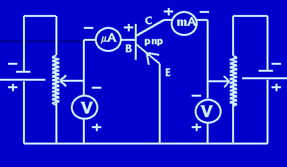
CIRCUIT DIAGRAM:-
PROCEDURE:-
a) Input Characteristics
Make the connections as shown in the circuit diagram.
The collector - emitter voltage VCE is kept constant at 0 V. The emitter - base voltage VEB
is varied in steps of 0.05 or 0.1 V and for each setting of the voltage, the current IB is noted.
The value of VCE is then set at 5 V and the above procedure is repeated.
The value of VCE is then set at 10 V and the above procedure is repeated again.
The reading are recorded in table 1.
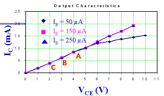
b) Output characteristics
The input current, i.e. base current, IB is kept constant at 50 microA. Voltage VCE
is varied in steps of 1 V from 0 to 10 V and for each setting of the voltage, the output current, i.e. collector current IC is noted.
For each new value of collector voltage, the base current is checked and adjusted to the value at which it is to be kept constant.
The value of IE is then set at 150 microA and the above procedure is repeated.
The value of IB is then set at 250 microA and the above procedure is again repeated.The readings are recorded in table 2.
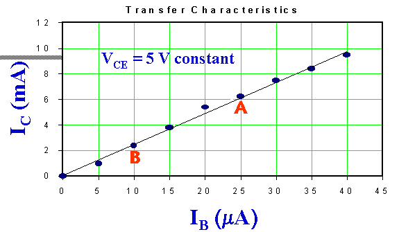
c) Transfer characteristics
The collector voltage VCE is kept constant at some value. Base current is varied in steps and corresponding collector current IC is noted and recorded in table 3.
OBSERVATIONS:-
|
VCE = 0 V |
VCE = 5 V |
VCE = 10 V |
|||
|
VBE V |
IB microA |
VBE V |
IB microA |
VBE V |
IB microA |
|
0 |
0 |
0 |
|||
|
IB = 50 microA |
IB = 150 microA |
IB = 250 microA |
|||
|
VCE V |
IC mA |
VCE V |
IC mA |
VCE V |
IC mA |
|
0 |
0 |
0 |
|||
VCE = constant at 5 V.
|
IB microA |
IC mA |
|
0 |
GRAPH:-
i) To draw input characteristics, VBE values are taken along x - axis and IB values are taken along y - axis and the graphs are plotted for all three constant VCE values.
ii) To draw outut characteristics, VCE values are taken along x - axis and IC values are taken along y - axis and the graphs are plotted for all three constant IB values.
iii) To draw transfer characteristics, IB values are taken along x - axis and IC values are taken along y - axis and the graph is plotted.
i) ri = [delta(VBE) / delta(IB)] at VCE = constant =
ii) ro = [delta(VCE) / delta(IC)] at IB = constant =
iii) betaDC = (IC) / (IB) at VCE = constant
iv) betaAC = [delta(IC) / delta(IB)] at VCE = constant =
RESULT:-
i) Input dynamic resistance, ri =
ii) Output dynamic resistance, ro =
iii) DC current gain, betaDC =
iv) AC current gain, betaAC =
PRECAUTIONS:-